- All products
- Prototyping
- Components
- ICs
- Logic Gates
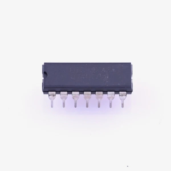
- Logic Gate NOT (Inverter) 74HC04
- Logic Gates
Features:
- Hex NOT Gate: Includes six independent inverter gates in one integrated circuit.
- Digital Logic Operation: Designed for standard binary logic inputs and outputs.
- CMOS Technology: Ensures low power consumption and high noise immunity.
- High Speed Performance: Suitable for fast switching digital applications.
- Wide Voltage Range: Operates reliably from 2V to 6V.
- Logic Compatibility: Works with both CMOS and TTL logic levels.
- Compact IC Package: Standard 14 pin package for easy integration.
- Low Output Impedance: Capable of driving multiple digital inputs.
- Temperature Stability: Reliable operation across a wide temperature range.
- Cost Effective: Simple and widely available inverter solution.
Principle of Work:
Each inverter within the 74HC04 performs a NOT operation. When the input is low, the output becomes high. When the input is high, the output becomes low. This operation follows the basic NOT gate truth table.
- A | Y
- 0 | 1
- 1 | 0
All six inverters operate independently and can be combined to build more complex digital logic circuits.
Pinout:
- Pin 1: Input 1
- Pin 2: Output 1
- Pin 3: Input 2
- Pin 4: Output 2
- Pin 5: Input 3
- Pin 6: Output 3
- Pin 7: GND Ground
- Pin 8: Output 4
- Pin 9: Input 4
- Pin 10: Output 5
- Pin 11: Input 5
- Pin 12: Output 6
- Pin 13: Input 6
- Pin 14: VCC Supply Voltage
Applications:
- Signal Inversion: Converts active high signals to active low and vice versa.
- Logic Level Control: Generates complementary control signals.
- Clock and Oscillator Circuits: Used in simple timing applications.
- Buffering: Isolates and protects digital circuit stages.
- Control Circuits: Adapts logic levels for sensors and switches.
- Educational Projects: Common in learning and training environments.
Technical Details:
- Supply Voltage: 2V to 6V
- Operating Temperature: -40 C to 85 C
- Propagation Delay: 11 ns typical at 5V
- Input Current: Plus or minus 20 mA
- Output Current: Plus or minus 5 mA
- Package Type: 14 pin DIP
Comparisons:
- Voltage Range: Wider operating voltage than traditional TTL inverter ICs.
- Power Consumption: Lower power usage due to CMOS design.
- Switching Speed: Faster response suitable for modern digital circuits.