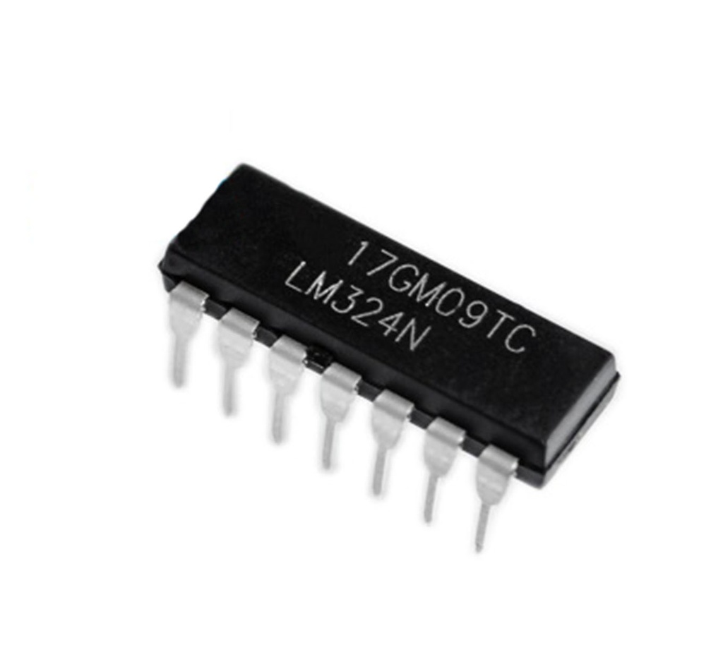
Features:
- 4 independent operational amplifiers in a DIP-14 package
- Short-circuit protection (on some variants)
- Internally frequency-compensated for unity gain
- True differential input stage
- Large DC voltage gain: 100 dB
- Wide bandwidth: 1 MHz (unity gain)
- Single-supply operation from 3V to 32V
- Input voltage range equals power supply range
- Output voltage swing from 0V to V+ − 1.5V
Principle of Work:
Operational amplifiers are multi-stage amplifiers packaged into a single integrated circuit. Each op-amp within the LM324 has two inputs — an inverting (-) and a non-inverting (+) — and a single output. The output signal’s phase depends on which input is used. If an input signal is applied to the inverting terminal, the output is 180° out of phase. If applied to the non-inverting terminal, the output remains in phase. The LM324 supports single or dual power supply configurations using pins 4 (Vcc) and 11 (Vee/GND).
Pinout:
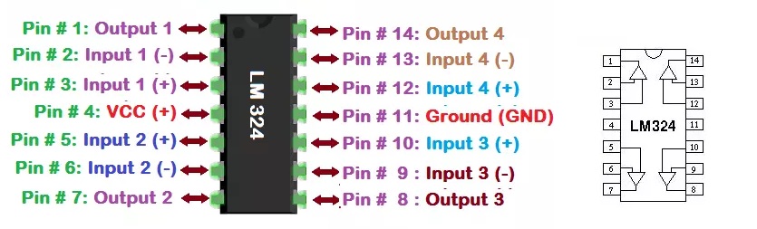
| Pin | Description |
|---|---|
| 1 | Output 1 |
| 2 | Inverting Input 1 |
| 3 | Non-inverting Input 1 |
| 4 | Vcc (Positive Supply) |
| 5 | Non-inverting Input 2 |
| 6 | Inverting Input 2 |
| 7 | Output 2 |
| 8 | Output 3 |
| 9 | Inverting Input 3 |
| 10 | Non-inverting Input 3 |
| 11 | Vee/GND (Negative Supply or Ground) |
| 12 | Non-inverting Input 4 |
| 13 | Inverting Input 4 |
| 14 | Output 4 |
Applications:
- Audio mixers and preamplifiers
- Voltage follower/buffer circuits
- DC gain blocks and signal conditioning
- Cell phone detectors and RF sensors
- Oscilloscopes, inverters, UPS systems
- Analog computing operations: summing, integration, differentiation
Circuit Example:
LM324 Cell Phone Detector Circuit
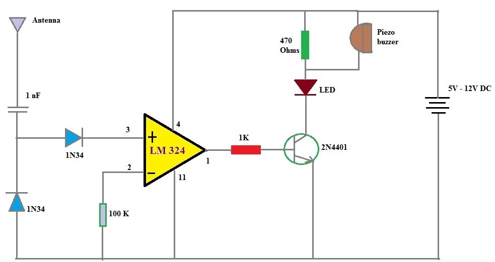
This simple circuit detects mobile phone signals in the 10–20m range. It activates a piezo buzzer and LED when RF activity is detected, useful for surveillance or signal detection applications.
Technical Details:
| Parameter | LM324 |
|---|---|
| Input Offset Voltage | 3 mV |
| Input Bias Current | 100 nA |
| Input Offset Current | 30 nA |
| Common Mode Voltage Range | -1.5V to Vcc |
| Voltage Gain | 100 V/mV |
| Supply Current | 3.0 mA |
| Common Mode Rejection Ratio | 85 dB |
| Supply Voltage | Up to 32V |
| Thermal Resistance | 88 °C/W (junction-to-ambient) |
| Power Dissipation (PDIP) | 1130 mW |
| Junction Temperature | 70°C |
Comparisons:
| Specification | LM358 | LM324 |
|---|---|---|
| Supply Voltage | Up to 32V | Up to 32V |
| Power Dissipation | 830 mW (DIP) | 1130 mW (DIP) |
| Input Offset Voltage | 5 mV | 5 mV |
| Offset Voltage Drift | 20 µV/°C | 30 µV/°C |
Resources:
Features:
- 4 independent operational amplifiers in a DIP-14 package
- Short-circuit protection (on some variants)
- Internally frequency-compensated for unity gain
- True differential input stage
- Large DC voltage gain: 100 dB
- Wide bandwidth: 1 MHz (unity gain)
- Single-supply operation from 3V to 32V
- Input voltage range equals power supply range
- Output voltage swing from 0V to V+ − 1.5V
Principle of Work:
Operational amplifiers are multi-stage amplifiers packaged into a single integrated circuit. Each op-amp within the LM324 has two inputs — an inverting (-) and a non-inverting (+) — and a single output. The output signal’s phase depends on which input is used. If an input signal is applied to the inverting terminal, the output is 180° out of phase. If applied to the non-inverting terminal, the output remains in phase. The LM324 supports single or dual power supply configurations using pins 4 (Vcc) and 11 (Vee/GND).
Pinout:
| Pin | Description |
|---|---|
| 1 | Output 1 |
| 2 | Inverting Input 1 |
| 3 | Non-inverting Input 1 |
| 4 | Vcc (Positive Supply) |
| 5 | Non-inverting Input 2 |
| 6 | Inverting Input 2 |
| 7 | Output 2 |
| 8 | Output 3 |
| 9 | Inverting Input 3 |
| 10 | Non-inverting Input 3 |
| 11 | Vee/GND (Negative Supply or Ground) |
| 12 | Non-inverting Input 4 |
| 13 | Inverting Input 4 |
| 14 | Output 4 |
Applications:
- Audio mixers and preamplifiers
- Voltage follower/buffer circuits
- DC gain blocks and signal conditioning
- Cell phone detectors and RF sensors
- Oscilloscopes, inverters, UPS systems
- Analog computing operations: summing, integration, differentiation
Circuit Example:
LM324 Cell Phone Detector Circuit
This simple circuit detects mobile phone signals in the 10–20m range. It activates a piezo buzzer and LED when RF activity is detected, useful for surveillance or signal detection applications.
Technical Details:
| Parameter | LM324 |
|---|---|
| Input Offset Voltage | 3 mV |
| Input Bias Current | 100 nA |
| Input Offset Current | 30 nA |
| Common Mode Voltage Range | -1.5V to Vcc |
| Voltage Gain | 100 V/mV |
| Supply Current | 3.0 mA |
| Common Mode Rejection Ratio | 85 dB |
| Supply Voltage | Up to 32V |
| Thermal Resistance | 88 °C/W (junction-to-ambient) |
| Power Dissipation (PDIP) | 1130 mW |
| Junction Temperature | 70°C |
Comparisons:
| Specification | LM358 | LM324 |
|---|---|---|
| Supply Voltage | Up to 32V | Up to 32V |
| Power Dissipation | 830 mW (DIP) | 1130 mW (DIP) |
| Input Offset Voltage | 5 mV | 5 mV |
| Offset Voltage Drift | 20 µV/°C | 30 µV/°C |