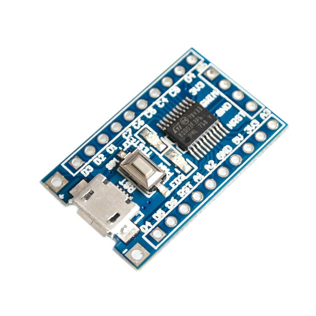
STM8S Core Board Main Features:
- Utilizes STM8S103F3P6 as the main IC
- Can be powered using a 2.54mm pin header or solder pads
- Input voltage range: 4.5V - 15V via pads; 3.3V output available via pin
- Note: The 5V pin reflects the input voltage directly
- All pins are broken out with clear labels next to each pin
- Includes reset button, power LED, and a user demo LED
- Compact size and well-designed layout
- Supports SWIM debug mode
Technical Information:
- Includes schematic in PDF format and test code
- Preloaded test program flashes the LED to verify proper function
- Supports both IAR and STVD development environments
- Includes register and library-based examples such as:
- Timer routine
- UART transmit and receive
- Clock switching
- ADC routines
- STM8 software libraries and tools included
- IAR development IDE and STVP programming tool supported
STM8S003F3P6 Performance Notes:
- 128 bytes EEPROM
- FLASH memory can be erased up to 100 times
- Board Dimensions: 28mm x 17mm x 5mm (1.1" x 0.66" x 0.19")
- Quantity: 1 piece
Board Features:
- SWIM Connector
- Voltage Regulator (3.3V - AMS1117)
- Micro USB connector for powering via smartphone charger or USB
- All pins accessible via headers
- Power LED indicator
- User LED connected to PB.5
- Reset switch included
Sample Code:
#include "stm8s.h"

void myDelay(void);

void myDelay() {
  int i, j;
  for (i = 0; i < 1000; i++) {
    for (j = 0; j < 100; j++);
  }
}

main() {
  GPIOB->DDR |= 0x20;       // PB.5 as Output
  GPIOB->CR1 |= 0x20;       // PB.5 as Push Pull Type Output

  while (1) {
    GPIOB->ODR |= 1 << 5;   // PB.5 = 1
    myDelay();
    GPIOB->ODR &= ~(1 << 5); // PB.5 = 0
    myDelay();
  }
}
Downloads:
- STM8S103F3P6 Schematics: STM8S103F3P6_Sch.png (423.24 KB)
- STM8S103F3P6 Board Layout: STM8S103F3P6_Layout.png (63.38 KB)