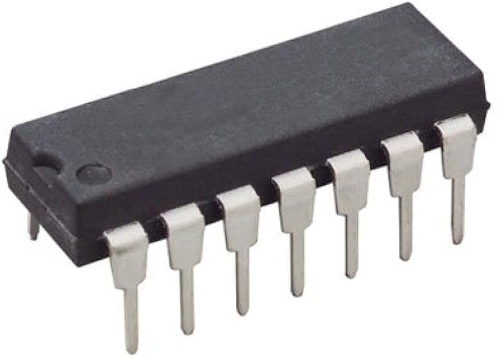
On the positive edge of a clock pulse, the flip-flop is activated. The status of the data pin (D) is collected and held as the output when the clock pin (CLK) turns high (Q). The output Q will not change again until the next clock rising edge, regardless of how long the clock remains high or if D changes.
Specifications:
- Output Drive Capability: 10 LSTTL Loads
- Outputs directly interface to CMOS, NMOS, and TTL
- Operating Voltage Range: 2.0 to 6.0 V
- Low Input Current: 1.0 μA
- High Noise Immunity characteristic of CMOS devices
- In compliance with the JEDEC Standard No. 7A requirements
The Truth Table for the D-type Flip-Flop:
| Clk |
D |
Q |
Q̅ |
Description |
| ↓ 0 |
X |
Q |
Q̅ |
Reminder, No change |
| ↑ 1 |
0 |
0 |
1 |
Reset Q → 0 |
| ↑ 1 |
1 |
1 |
0 |
Set Q → 1 |
How Does a D Flip-Flop Work:
The device includes preset and clear inputs, which can drive Q high or low, but they are not used in this instance. Since preset and clear are actuated by a low signal, they are connected to Vcc to keep them high. The IC also provides an inverted output (Q̅), which is always the inverse of Q, though it is not utilized here.
In this case, the SN74HC74 is simple to operate; only clock and data signals are required. However, the flip-flop is sensitive to noise since it responds to the rising edge of the clock signal. A mechanical switch is employed instead of a pure electrical closure in this example.
