The device can be used in shift registers, counters, and toggle applications by connecting the "Q" output back to the data input. On the rising edge of the clock pulse, the logic level at the "D" input is transferred to the Q output. Set and reset operations work independently of the clock by applying a HIGH level to the respective set or reset inputs.
What is a D Flip-Flop?
A D flip-flop is a bistable circuit that stores one bit of information (HIGH or LOW). When the clock signal transitions from LOW to HIGH (rising edge), the output takes the value present on the D (data) input.
Specifications
- Wide supply voltage range: 3.0V to 15V
- High noise immunity: 0.45 VDD
- Low power TTL compatibility: fan-out of 2 (driving 74L) or 1 (driving 74LS)
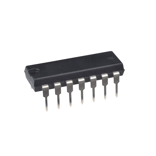
- Package Type: DIP
Pinout of the CD4013
| Pin Name |
Pin Number |
Type |
Description |
| VDD |
14 |
Power |
Supply Voltage (+3V to +15V) |
| GND |
7 |
Power |
Ground (0V) |
| Q1, Q2 |
1, 13 |
Output |
Outputs of the two D Flip-Flops |
| Q̅1, Q̅2 |
2, 12 |
Output |
Inverted outputs of the two D Flip-Flops |
| CLK1, CLK2 |
3, 11 |
Input |
Clock input (rising edge) for the two flip-flops |
| D1, D2 |
5, 9 |
Input |
Data input for the two flip-flops |
| S1, S2 |
6, 8 |
Input |
Set (preset output to 1) |
| C1, C2 |
4, 10 |
Input |
Reset (clear output to 0) |
Applications
- Automotive electronics
- Alarm systems
- Data terminals
- Industrial electronics
- Instrumentation
- Remote metering
- Medical electronics
- Computers
The device can be used in shift registers, counters, and toggle applications by connecting the "Q" output back to the data input. On the rising edge of the clock pulse, the logic level at the "D" input is transferred to the Q output. Set and reset operations work independently of the clock by applying a HIGH level to the respective set or reset inputs.
What is a D Flip-Flop?
A D flip-flop is a bistable circuit that stores one bit of information (HIGH or LOW). When the clock signal transitions from LOW to HIGH (rising edge), the output takes the value present on the D (data) input.
Specifications
- Wide supply voltage range: 3.0V to 15V
- High noise immunity: 0.45 VDD
- Low power TTL compatibility: fan-out of 2 (driving 74L) or 1 (driving 74LS)
- Package Type: DIP
Pinout of the CD4013
| Pin Name |
Pin Number |
Type |
Description |
| VDD |
14 |
Power |
Supply Voltage (+3V to +15V) |
| GND |
7 |
Power |
Ground (0V) |
| Q1, Q2 |
1, 13 |
Output |
Outputs of the two D Flip-Flops |
| Q̅1, Q̅2 |
2, 12 |
Output |
Inverted outputs of the two D Flip-Flops |
| CLK1, CLK2 |
3, 11 |
Input |
Clock input (rising edge) for the two flip-flops |
| D1, D2 |
5, 9 |
Input |
Data input for the two flip-flops |
| S1, S2 |
6, 8 |
Input |
Set (preset output to 1) |
| C1, C2 |
4, 10 |
Input |
Reset (clear output to 0) |
Applications
- Automotive electronics
- Alarm systems
- Data terminals
- Industrial electronics
- Instrumentation
- Remote metering
- Medical electronics
- Computers